
Process Introduction
From circuit formation to final visual inspection, we operate an in-line production system that handles all 14 process steps on a single line.
-
01
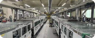
Pattern (Dry Film)
A process for circuit formation. After lamination, the required areas of the coated D/F are photo-cured with a laser, and the circuit is then formed through etching.
-
02
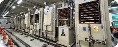
Hot Press
A process that melts and cures the Pre-Preg through heat and pressure to bond the copper foil and inner-layer core, creating a multilayer board.
-
03
Drill (CNC)
A process that machines holes for the inter-layer conduction (PTH) and component mounting required between each layer.

-
04
Laser Drill
A process that machines Micro-Via holes with a laser beam to form inter-layer connections.

-
05
Copper Plating / Via Fill
A process that applies chemical and electrical copper plating to the machined holes (PTH, Micro-Via) to achieve electrical conduction.

-
06
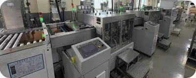
Hole Plugging
A process that fills epoxy resin ink inside the copper-plated PTH to ensure hole reliability.
-
07
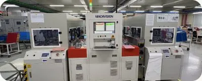
AOI
A process that detects defects in the formed circuit through automated optical inspection.
-
08
PSR
A process that applies insulating PSR ink to prevent oxidation of the formed circuit and solder bridges during component mounting.

-
09
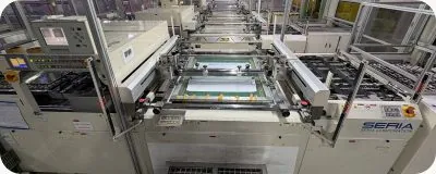
Marking
A process that prints the symbols and markings required for SMT component mounting.
-
10
Surface Finish / ENIG
A process that applies nickel and gold plating to reduce corrosion, wear and contact resistance of component-mounting pads and to improve solderability.

-
11
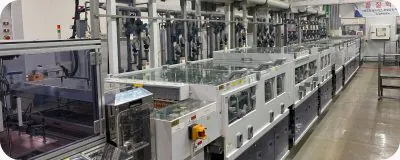
Surface Finish / OSP
Prevents oxidation by coating an organic film over the component-mounting pads.
-
12
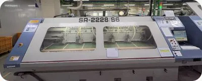
Router
A process that machines the outline to form the final product shape and size requested by the customer from the working panel.
-
13
BBT
A process that applies electrical resistance to the PCB bare board to inspect the circuits and holes for any abnormalities.

-
14
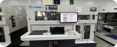
AFVI / Visual Inspection
A process that inspects the PCB's external quality through 100% inspection before shipment to the customer.